

L’AV143 fait partie de la gamme de solutions de conversion de données et de traitement du signal à haut débit d’apissys basées sur la norme VITA 46, VPX.
L’AV143 est entièrement conforme à la norme OpenVPX, prenant en charge divers protocoles de communication tels que PCIe, SRIO, 1 Gbit et XAUI 10 Gbit Ethernet, ainsi que des normes non adoptées par OpenVPX telles que Aurora.
L’AV143 combine un DAC double canal 12 bits 3,2 Gsps / un seul canal 12 bits 6,4 Gsps et un DAC double canal 12 bits 3,2 Gsps / monocanal 12 bits 6,4 Gsps avec une puissance de traitement ultra-élevée fournie par le FPGA Xilinx® Virtex® Ultrascale+™, ce qui le rend parfaitement adapté aux applications de traitement du signal embarqué telles que la guerre électronique, émetteurs/récepteurs radar à large bande ou applications de communication à large bande.
L’AV143 dispose d’une référence interne à très faible gigue et d’un synthétiseur d’horloge et peut être utilisé avec une horloge externe ou une référence externe pour une plus grande flexibilité.
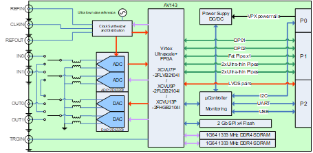
L’AV143 comprend un FPGA Xilinx® Virtex® Ultrascale+ ™ VU13P pour une capacité de traitement impressionnante de plus de 19 TMAC (Multiply Accumulate per second), deux mémoires SDRAM DDR4-2666 1G64 pour le traitement des données et une mémoire FLASH synchrone de 2 Go pour le stockage de plusieurs micrologiciels. L’AV143 peut également être équipé d’un FPGA Xilinx® Virtex® Ultrascale+ ™ VU7P ou VU9P.
L’AV143 fournit une interface USB 2.0 et une interface USB vers UART destinée à être utilisée pour la surveillance et la supervision du système.
L’AV143 est livrée avec des pilotes logiciels complets pour Windows et Linux. Un kit de développement FPGA est fourni, comprenant tous les cœurs nécessaires à la création d’une application FPGA utilisateur.
Analog Inputs/Outputs• Input coupling: AC • Full power bandwidth: > 8 GHz • Full scale : TBD dBm • Output coupling: AC • Full power bandwidth: > 8 GHz • Full scale : TBD dBm (NRZ) • Impedance: 50 Ohm • Connectors: SMPM
| Trigger• External: 0 to 2.5Vp • Connector: SMPM, 50 Ohm
| Software support• Software Drivers • Windows 10 64-bits • Linux 64-bits
|
12-bit 3.2/6.4 Gsps ADC
The AV143 Analog to Digital conversion is performed by one Texas Instruments ADC12DL3200 12-bit 3.2/6.4 Gsps ADC
The AV143 provides two front panel SMPM connectors for analog input.
Single ended input signals are AC coupled with an input bandwidth from 10 MHz to more than 8 GHz with TBD dBm input level.
12-bit 3.2/6.4 Gsps DAC
The AV143 Digital to Analog conversion is performed by one Texas Instruments DAC12DL3200 12-bit 3.2/6.4 Gsps DAC.
The AV143 provides two front panel SMPM connectors for analog output.
Single ended output signals are AC coupled with an output bandwidth from 10 MHz to more than 8 GHz with TBD dBm output level (NRZ).
Clock
The AV143 provides one ultra-low jitter clock synthesizer locked on a 100 MHz internal reference. The AV143 supports a 10 to 500 MHz external reference input from a front panel SMPM connector. A reference output is available on a front panel SMPM connector.
An external clock input for the ADC and DAC is supported from one front panel SMPM connector.
External clock frequencies from 1.6 GHz to 6.4 GHz are supported.
Trigger and Synchronization
The AV143 provides one front panel SMPM connector for external trigger input.
FPGA
The AV143 is fitted with a Xilinx® Virtex® Ultrascale+™ VU7P, VU9P or VU13P user programmable FPGA. Only few resources are used to control and communicate with external hardware such as DDR4 SDRAM and monitoring sub-system, leaving most of the logic and block RAM and all DSP resources available for customer processing.
Dedicated to signal processing, the Xilinx Virtex Ultrascale+ VU13P FPGA includes 3,780 K logics cells, 94.5 Mbit of RAM blocs, 360 Mbit of Ultra RAM, 4 PCIe GEN3x16 interface blocs and 12,288 DSP48 slices for an impressive processing power of more than 19 TMACs.
The FPGA is delivered in -2 speed grade.
Memories
The AV143 includes two 1G64 DDR4-2666 SDRAM memory banks and one 2 Gbit QSPI FLASH used to store multiple FPGA configuration files.
VPX interface
The AV143 features an OpenVPX VITA 65 compliant interface with support for two Fat Pipes for Data Plane, one Fat Pipe for Expansion Plane, two Ultra-Thin Pipes for Control Plane and two User Defined Ultra-Thin Pipes on P1. The AV143 also supports 22 LVDS differential pairs configurable as 44 single-ended LVCMOS on P2 plus USB2.0 and UART for supervision and monitoring.
The AV143 features one low phase noise clock generator able to synthesize clock references for the FPGA GTYs from 60 MHz to 820 MHz, allowing support of all major protocols such as Aurora, GigE, PCIe Gen 1, 2 and 3 and XAUI 10Gbit Ethernet up to 28 Gbps.
Microcontroller
The AV143 features a 32-bit 200 MHz microcontroller used primarily for board monitoring and supervision.
The microcontroller supports a USB 2.0 and a UART interfaces accessible on the VPX P2 user IO pins through an ApisSys AR113 Rear Transition Module.
The microcontroller firmware includes all necessary features for board monitoring and supervision.
Firmware
The AV143 comes with a firmware package which includes VHDL cores allowing for control and communication with all AV143 hardware resources.
A base design is provided which demonstrates the use of the AV143 and gives users a starting point for firmware development. The AV143 firmware package is supported on the Xilinx VIVADO® 2022.1 design suite.
Software
The AV143 is delivered with software drivers for Windows 10 and Linux.
Ruggedization
The AV143 is delivered in air cooled and conduction cooled standard or rugged versions for use in severe environmental conditions.
Standard VITA 47 ruggedization levels supported are EAC4, EAC6, ECC3 and ECC4.
| Part Number | A | V | 143 | - | rr | - | a | |
|---|---|---|---|---|---|---|---|---|
| Ruggedization level | Air Standard Air Rugged Conduction Standard Conduction Rugged | - - - - | - - - - | - - - - | - - - - | AS AR CS CR | - - - - | - - - - |
| Options | FPGA Virtex Ultrascale+ VU7P FPGA Virtex Ultrascale+ VU9P FPGA Virtex Ultrascale+ VU13P | - - - | - - - | - - - | - - - | - - - | - - - | 7 9 13 |
| Air flow, Standard AS (VITA 47 EAC4) | Air flow, Rugged AR (VITA 47 EAC6) | Conduction Standard CS (VITA 47 ECC3) | Conduction Rugged CR (VITA47 ECC4) | |
|---|---|---|---|---|
| Operating Temperature | 0°C to +55°C (1) (10 CFM airflow at sea level) | -40 to +70ºC (1) (20 CFM airflow at sea level) | -40°C to +70°C (Card Edge) | -40°C to +85°C (Card Edge) |
| Non Operating Temperature | -40°C to +85°C | -50°C to +100°C | -50°C to +100°C | -55°C to +105°C |
| Operating Vibration (Random) | 5Hz - 100Hz +3 dB/octave 100Hz-1kHz = 0.04 g2/Hz 1kHz - 2kHz -6 dB/octave | 5Hz - 100Hz +3 dB/octave 100Hz - 1kHz = 0.04 g2/Hz 1kHz - 2kHz -6 dB/octave | 5Hz - 100Hz +3 dB/octave 100Hz - 1kHz = 0.1 g2/Hz 1kHz - 2kHz -6 dB/octave | 5Hz - 100Hz +3 dB/octave 100Hz - 1kHz = 0.1 g2/Hz 1kHz - 2kHz -6 dB/octave |
| Operating Shock | 20g, 11 millisecond, half-sine | 20g, 11 millisecond, half-sine | 40g, 11 millisecond, half-sine | 40g, 11 millisecond, half-sine |
| Operating Relative Humidity | 0% to 95% non-condensing | 0% to 95% non-condensing | 0% to 95% non-condensing | 0% to 95% non-condensing |
| Operating Altitude | @ 0 to 10,000 ft with adequate airflow | @ 0 to 30,000 ft with adequate airflow | @ 0 to 30,000 ft | @ 0 to 60,000 ft |
| Conformal Coating | No | Optional (default acrylic AVR80) | Yes (default acrylic AVR80) | Yes (default acrylic AVR80) |
ECCN number: 3A002h1